Programing the Flash memory:
31-Aug-2024
Using a blank PCB, I populated the 3.3V regulator and the Flash memory chip.
Then connected a QTPy board to the programing pins.
I wrote a Python program on my laptop which sends commands/data to the micro via the micros virtual serial port.
The micro then uses the SPI protocol to program the Flash memory on my board.
My first attempt to program the QTPy using its native python worked only just.
I kept having trouble with running out of memory. I think the python interpreter was itself using too much memory.
I also hadn't finished with other things the micro needed to do. So this was unlikely to work fully.
So for my second attempt I switched to using the Arduino system.
This proved much more successful. The current C code works well.
It isn't finished yet, there are more things it needs to do, like controlling the FPGA reset signal.
The code uses a simple Finite State Machine to control its operation.
The Python program that controls the micro isn't finished yet.
It can only program page 0 of the Flash memory with a pre-defined page of data. And read that page back.
When sending a page to the micro it sends a 16 bit CRC code as well, this is used by the micro to make sure that the
data received is exactly what was sent.
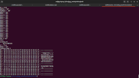 This is the program
output. The first page dump is what is going to be writen. Then there is the output of, first erasing the Flash and then writing the page to the
micro. And last is a dump of what is read from the Flash of page 0.
This is the program
output. The first page dump is what is going to be writen. Then there is the output of, first erasing the Flash and then writing the page to the
micro. And last is a dump of what is read from the Flash of page 0.
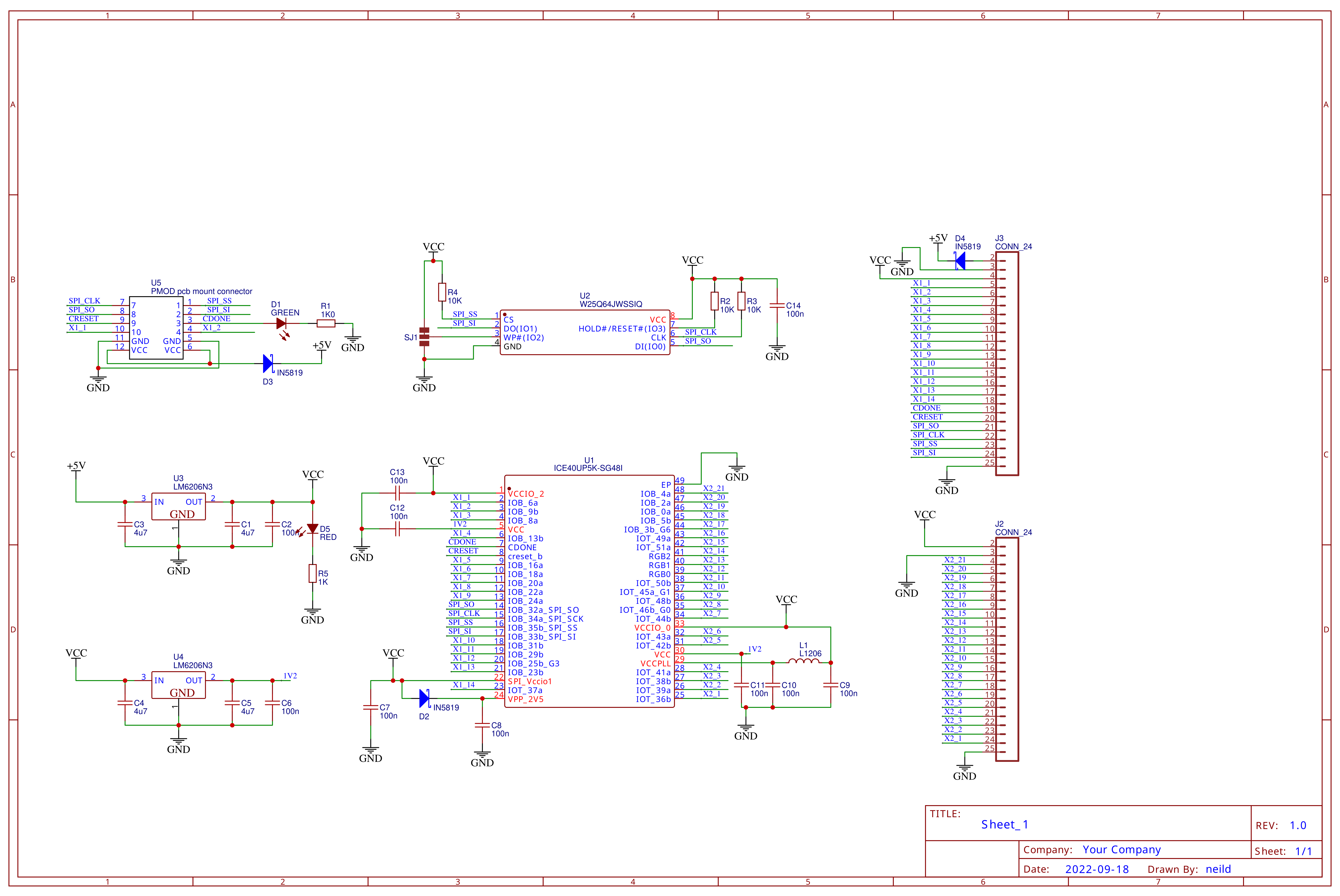 Circuit Diagram
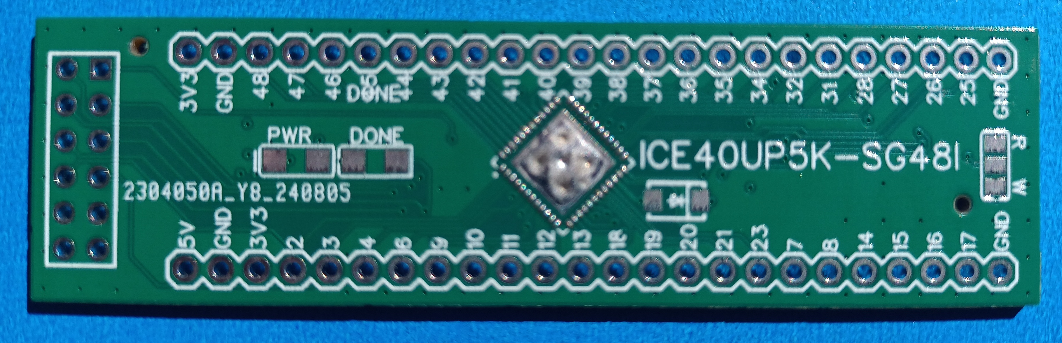 PCB Top
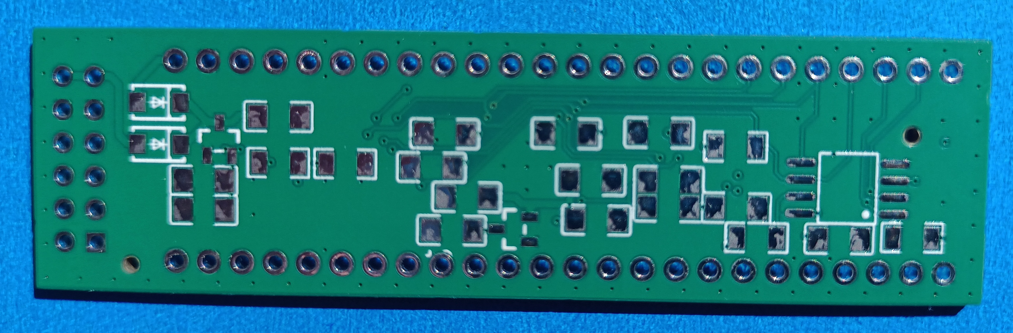 PCB Bottom